NEUCHÂTEL, Switzerland, June 14, 2018 — Researchers at the Swiss Center for Electronics and Microtechnology (CSEM) have developed an inkjet printing technique that can be used to print optical components, such as waveguides. The printing approach can also fabricate electronics and microfluidics.
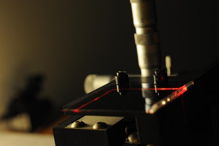
Researchers used an inkjet printing method to create the waveguide shown here. Sending laser light through the waveguide (red) allowed them to measure the waveguide's optical properties. Courtesy of Fabian Lütolf, CSEM.
"Inkjet printing is a very attractive method for fabricating optical components because the positions and sizes of features can easily be modified and there is virtually no material waste," said CSEM researcher Fabian Lütolf. "However, the surface tension of the inks makes it difficult to print lines with a specific height, which is necessary to create a waveguide."
Used as an additive manufacturing technique, inkjet printing uses tiny nozzles like the ones found in desktop inkjet printers to deposit a computer-generated pattern of drops onto a substrate to build a structure.
The researchers discovered that depositing the ink in two steps, rather than the traditional single step, enabled printing of lines with a specific height and with much smoother features than traditional techniques.
The CSEM technique can be used to print 2.5D optical waveguides and tapers made of acrylic polymer. The printing concept can also be used with other materials, such as metallic inks, to make electronics or sucrose mixtures for biodegradable applications.
"The fact that our approach could allow components with multiple functionalities to be fabricated with a single printer paves the way toward additive manufacturing of entire integrated circuits on chips," said Lütolf. "This means that optical components could be added to flexible hybrid electronics and that optoelectronic components such as light sources or detectors could be integrated into printed optical circuits."
The technique offers several advantages over classical photolithography, which is typically used to make tiny components on chips.
"Inkjet printing doesn't require a physical mask like photolithography and it is easier to connect components," said Lütolf. "Also, if you just want to quickly test an idea or vary a parameter, additive manufacturing methods such as inkjet printing only require adaption of the digital design."
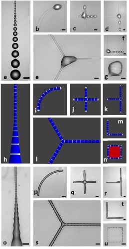
A comparison of printed features with the standard, one-step inkjet printing (a-g), as theoretically calculated for the new two-step inkjet printing method (h-n), and the actual print thereof (o-u). Scale bars = 200 μm. Courtesy of Fabian Lütolf, CSEM.
To evaluate the new printing method, the researchers created a polymer waveguide that was 120 μm wide and 31 μm tall with a taper that allowed light from an external laser source to enter the waveguide. They measured the optical loss within the waveguide to be 0.19 dB/cm, only an order of magnitude higher than state-of-the-art waveguides created using photolithography.
According to the researchers, the smallest possible waveguides consist of a single droplet of ink, the size of which is limited by the nozzle of the inkjet printer. For the printer used in the study, the narrowest waveguides would be in the 40-μm range with a height of around 10 μm. Typical industrial inkjet printers also have similar limits.
The CSEM researchers are working to optimize the printing method and the ink to further lower the amount of light lost by the waveguide. They also plan to make the inkjet process more applicable for large-scale fabrication and commercial implementation.
The research has been published in the journal Optics Express (doi.org/10.1364/OE.26.011934).
By photonics.com June 2018